
What is PCB Flying Probe Testing?
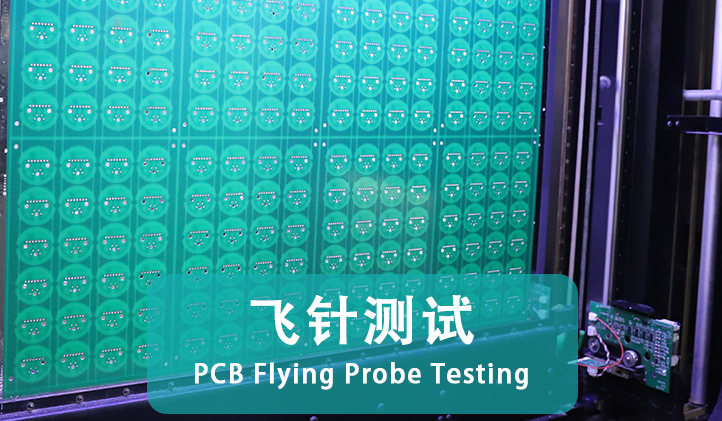
Flying probe testing is an electrical testing method used in the PCB Manufacturing process, primarily for detecting open circuits, short circuits, and other electrical defects that may occur during production. The basic principle involves multiple probes that can move freely along the X, Y, and Z axes. Under computer control, these probes sequentially contact various test points on the PCB to perform comprehensive checks on conductivity and electrical performance.
In terms of testing effectiveness, flying probe testing offers several advantages, including high precision, the ability to cover complex and densely routed areas, and no reliance on fixed test point layouts. The test accuracy typically reaches the micrometer level. Using two or more high-speed moving probes, the system automatically contacts the pads or test points on the PCB according to a predefined program and measures parameters such as resistance, voltage, and current to determine whether the circuitry is functioning properly.
As a result, flying probe testing can efficiently detect common electrical defects such as open circuits, short circuits, and cold solder joints, without the need for customized test fixtures. With its high accuracy, flexibility, and adaptability, it has become an indispensable inspection method in PCB manufacturing—particularly valuable during sample verification, small-batch production, and new product development stages.