
The Impact of Flatness on PCBs
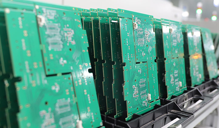
In the PCB manufacturing process, flatness is a critical factor affecting the quality and performance of circuit boards. It not only influences the soldering quality of electronic components but also directly impacts the reliability of product assembly and electrical performance. As electronic products move toward higher density, faster speeds, and greater reliability, controlling PCB flatness has become an essential aspect of both manufacturing and design.
First, flatness is crucial for component assembly. In surface-mount technology (SMT), if a PCB is warped or deformed, the contact between components and pads may be uneven, leading to soldering defects such as cold joints, false soldering, or tombstoning. On automated pick-and-place production lines, a flat PCB ensures that components are accurately picked up and placed, improving production efficiency and assembly precision. Conversely, warped boards may result in component misalignment or missing placements, affecting production line stability and yield.
Second, flatness affects product installation and fixation. For PCBs with edge connectors (such as gold fingers), poor flatness can cause connectors to fit improperly, leading to intermittent contact or signal loss. During overall product assembly, a flat PCB fits precisely with the chassis, brackets, and fastening elements (screws, clips, etc.), ensuring structural stability and reducing the risk of loosening or damage caused by board warping, thereby improving long-term reliability.
Finally, flatness has a significant impact on electrical performance. Especially in high-frequency and high-speed applications, an uneven PCB surface can alter signal path lengths and impedance consistency, resulting in signal reflection, crosstalk, and increased transmission loss. Additionally, warped or deformed PCBs are prone to stress under thermal cycling or long-term use, which may cause solder joint cracking or delamination, reducing the overall reliability of the circuit board.