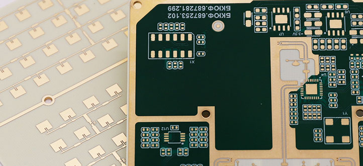
What is the process of PCB manufacturing?

What is the process of PCB manufacturing? PCBs are used in almost all electronic products, from small items like watches and headphones to larger applications such as military and aerospace. Despite their widespread use, most people are unfamiliar with how PCBs are produced. In the following, let's understand the PCB production process and its steps!
The PCB fabrication process can be roughly divided into the following twelve steps, each of which involves various processing techniques. It's important to note that different board structures may have different processes. The following process outlines the complete fabrication process for multi-layer PCBs.
Step One: Inner Layers
The main purpose here is to create the internal circuitry of the PCB:
1. Material Cutting: Cut the PCB substrate to the production size.
2. Pre-treatment: Clean the surface of the PCB substrate to remove contaminants.
3. Dry Film Lamination: Apply dry film to the PCB surface for subsequent image transfer.
4. Exposure: Use UV light to expose the dry film and transfer the image onto it.
5. Development and Etching (DE): Develop, etch, and remove the dry film to complete the inner layer fabrication.
Step Two: Inner Inspection
Primarily for testing and repairing the board's circuits:
1. Automated Optical Inspection (AOI): Use AOI to compare the PCB image with data from good boards to identify defects.
2. Visual Repair Station (VRS): Defects detected by AOI are sent to VRS for repair.
3. Wire Repair: Solder wires onto gaps or depressions to ensure electrical connectivity.
Step Three: Lamination
This step involves pressing multiple inner layers together:
1. Brown Oxide Treatment: Increases adhesion between the board and resin and improves copper surface wettability.
2. Riveting: Cut PP into small and normal sizes for layer alignment.
3. Layer Stacking, Pressing, Target Drilling, Beveling, and Edge Grinding:**
Step Four: Drilling
Drill holes of different sizes as per customer requirements for component installation, interconnections, and improved heat dissipation.
Step Five: First Copper
Copper plating the holes of the outer layer boards to establish circuit continuity:
1. Deburring: Remove burrs around the holes to prevent poor copper plating.
2. Resin Removal: Clear resin residues from the holes to enhance adhesion during micro-etching.
3. Through-hole Plating (PTH): Plate the holes with copper for inter-layer connectivity and increased copper thickness.
Step Six: Outer Layer
Similar to Step One but for the outer layers, facilitating further processing:
1. Pre-treatment: Acid wash, scrub, and dry the board to enhance dry film adhesion.
2. Dry Film Lamination: Apply dry film to the outer layer for image transfer preparation.
3. Exposure: UV exposure to create polymerized and unpolymerized areas on the dry film.
4. Development: Dissolve the unpolymerized dry film, leaving gaps.
Step Seven: Second Copper and Etching
Secondary copper plating followed by etching:
1. Secondary Copper Plating: Electroplate copper where dry film was not present.
2. Selective Etching System (SES): Remove the wet film attachment area's bottom copper through stripping, etching, and desoldering, completing outer layer circuitry.
Step Eight: Solder Mask (SMT)
Apply solder mask to protect the PCB and prevent oxidation:
1. Pre-treatment: Clean and roughen the copper surface for improved solder mask adhesion.
2. Screen Printing: Apply solder mask ink to non-soldering areas for protection and insulation.
3. Pre-baking: Remove solvent from solder mask ink and cure it for exposure.
4. Exposure: UV exposure to polymerize the solder mask ink into a high-molecular polymer.
5. Development: Remove unpolymerized solder mask ink using sodium carbonate solution.
6. Post-baking: Fully cure the solder mask.
Step Nine: Legend Printing
Print identification marks on the PCB:
1. Acid Washing: Clean the board's surface to enhance ink adhesion.
2. Screen Printing: Print marks for easy follow-up soldering.
Step Ten: Surface Finish - OSP (Organic Solderability Preservatives)
Apply a layer of organic material to prevent rust and oxidation on the exposed copper surface of the PCB.
Step Eleven: Shaping
Cut the board to the desired shape required by the customer for subsequent SMT assembly.
Step Twelve: Flying Probe Testing
Test the PCB's circuitry to prevent faulty boards from being shipped.
Step Thirteen: Final Quality Control (FQC)
Conduct final inspections after completing all processes.
Step Fourteen: Packaging and Shipping
Vacuum-pack the finished PCBs and ship them to customers, completing the delivery

